
Business·Tech
What is an EUV pellicle?
A critical semiconductor component in the form of an ultra-thin membrane, designed to protect costly EUV masks from particle contamination. It lets light pass through while keeping particles out of focus, so that contaminants landing on the mask surface are not transferred onto the wafer.
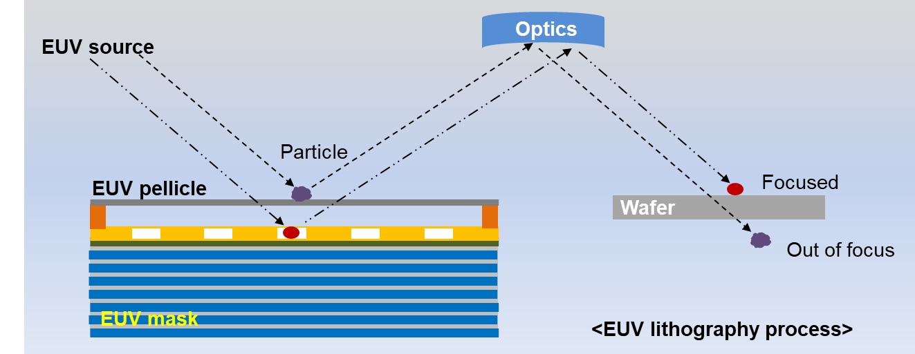
EUV Pellicle Structure
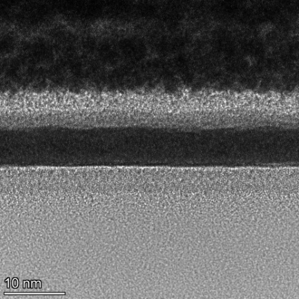
Tri-layer ultra-thin membrane under 20nm
The pellicle membrane consists of a tri-layer structure, with a total thickness of under 20nm. It is designed to transmit as much extreme ultraviolet light as possible while simultaneously securing mechanical durability and thermal stability.
How an EUV pellicle is made
Si-based pellicle manufacturing process — a 6-step flow that starts from a wafer and leaves only the ultra-thin membrane
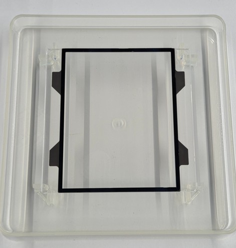
Pellicle-Frame Assembly
We combine our in-house developed pellicle and frame to build the completed assembly.
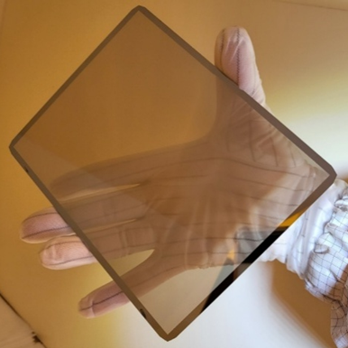
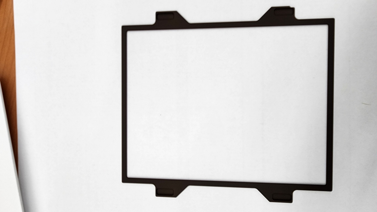
S&S TECH Pellicle Performance
| Category | Item | Measured value |
|---|---|---|
| Membrane · Optical | Transmittance | 92 ± 0.5 % |
| Reflectance | 0.015 ± 0.005 % | |
| Membrane · Mechanical | Tensile strength (UTS) | 2.4 ± 0.2 GPa |
| Rupture pressure | 50 ± 5 Pa | |
| Reliability | Lifetime | 25K wafers @ 500W |
| Membrane out-gassing (RBS) | No change | |
| Defectivity | No particles ≥ 10 µm | |
| Frame (in-house developed) | Out-gassing | Pass |
| Acceleration | 35 G |
* The figures above are representative values based on our own measurements; product specifications may vary depending on customer requirements and process conditions.