HomeBusiness·TechBlankmask
BLANKMASK

Where semiconductors
begin, drawn with light —
Blankmask

The first canvas of semiconductor micro-processing.
Circuit precision is determined on the purest substrate.
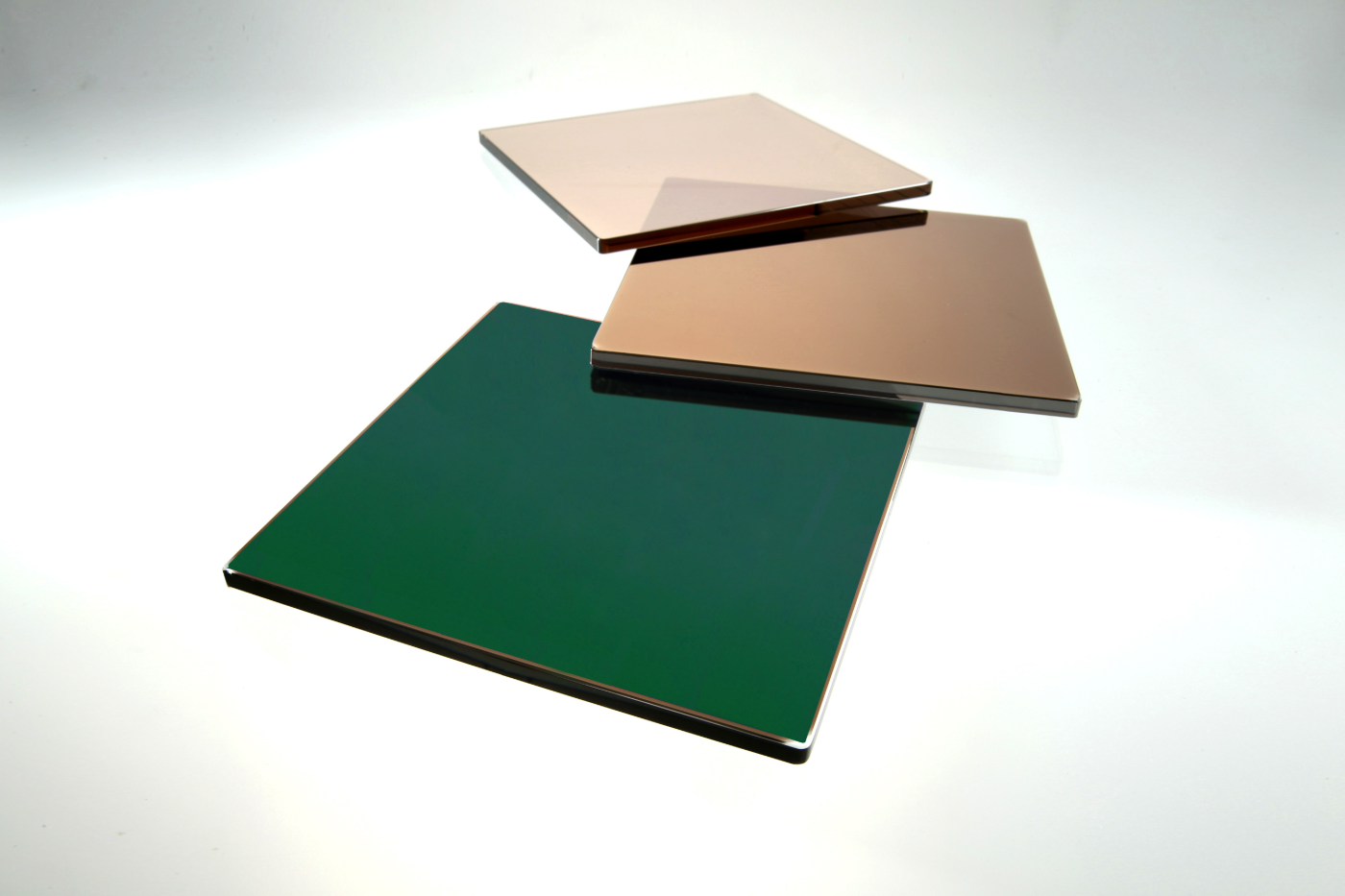
Blankmask — ultra-flat quartz substrate
QUARTZ SUBSTRATE
EASY GUIDE

What is a blankmask?

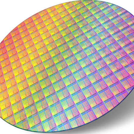
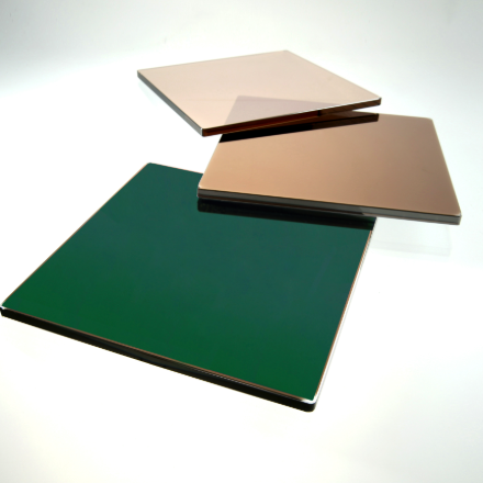
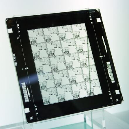
In a word, it is a "clean film before the photo is taken." Etching a semiconductor circuit design onto this film creates a photomask, and that design is copied onto the wafer with light to make a semiconductor.
Blankmask
Blankmask
A pristine substrate with no pattern yet
Photomask
Photomask
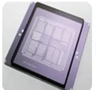
The "master film" with the circuit design etched onto it
Lithography
Lithography
Light transfers the design onto the wafer
Semiconductor Chip
Semiconductor Chip
The finished semiconductor with completed circuitry
HOW IT WORKS

How a blankmask is made

A circuit pattern is etched into a three-layer thin-film substrate to make a photomask, and that pattern is copied onto the wafer with light.

01

Blankmask cross-section

A substrate built from three layers of film.

Resist filmLight-sensitive filmMetal filmWhere the pattern is etchedQuartz substrateTransparent, ultra-flat base
02

Pattern formation

The circuit design is etched using light and chemical processes.

1
LithographyThe circuit design is drawn with light
2
Develop · EtchUnneeded film is etched away
3
Resist stripThe photoresist is washed off
Photomask with the light-blocking pattern
03

Transferring the circuit to the wafer

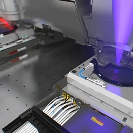
The finished photomask is mounted in the lithography system, and light transfers the circuit onto the wafer.

Photomask (master)Scanner(shrinks · focuses light)Circuit transferred to the silicon wafer
Terms made simpleLithographythe process of etching circuits with lightEtchingthe process of removing unneeded filmResista photosensitive film that reacts to light
PRODUCT LINE

Two kinds of light, two kinds of blankmask

Drawing semiconductors ever smaller requires light of shorter wavelength. The mask structure changes with the type of light.

DUV Blank Mask
Transmits · blocks light
A structure that transmits light193nm ArF · 248nm KrFQuartzCr filmWafer (only transmitted light forms the pattern)
Light (wavelength)193nm ArF · 248nm KrF
How it worksTransmits and blocks light
Substrate · thin filmHigh-purity quartz substrate + chrome-based film · phase-shift film
Applications
MemoryLogic (System IC)Power semiconductorsImage sensors
EUV Blank Mask
A structure that reflects light
NEXT-GEN
A structure that reflects light13.5nm EUVMo/SiMultilayerAbsorberCircuit from reflected light
Light (wavelength)13.5nm extreme ultraviolet (about 1/5,000 the width of a human hair)
How it worksReflects light (designed as a reflective structure since EUV cannot pass through glass or air)
Substrate · thin filmLow-thermal-expansion substrate + Mo/Si multilayer reflective film + capping layer + absorber layer
Quality controlNanometer-level defect control
Applications
AI semiconductorsHigh-performance logicNext-gen foundryHigh-density memory
BUSINESS AREA

Two business areas

The same blankmask technology becomes the starting point for two industries — semiconductors and displays.

SEMICONDUCTOR

For Semiconductors

Semiconductor masks that lead to fine circuitry on the wafer — from memory to AI logic.
BlankMask
BlankMask
Photo Mask
Photo Mask
Process
Process
Semiconductor
Semiconductor
View products
DISPLAY (FPD)

For Displays

Display masks that lead to large flat-panel circuitry — the foundation of high-resolution screens.

BlankMask
BlankMask
Photo Mask
Photo Mask
Process
Process
Display Panel
Display Panel
View products
IN YOUR LIFE

The technology that builds
the digital world, unseen
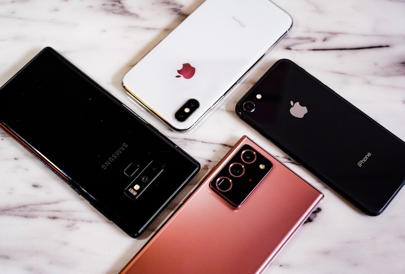
Smartphones
Smartphones
Automobiles
Automobiles
AI Servers
AI Servers
Data Centers
Data Centers
Nanometer-scale precision on a palm-sized 6-inch substrate